The different wiring methods can affect the distributed capacitance of transformer windings, which directly affects the performance of transformers. In this article, we will focus on the parameter of transformers.
The distributed capacitance of a transformer is a parasitic capacitance formed due to the presence of potential differences. It is a widely present electrical parameter, where there is distributed capacitance between two insulators as long as there is a voltage difference. Distributed capacitance has little impact on circuits at low frequencies, but its effects must be considered at high frequencies.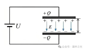
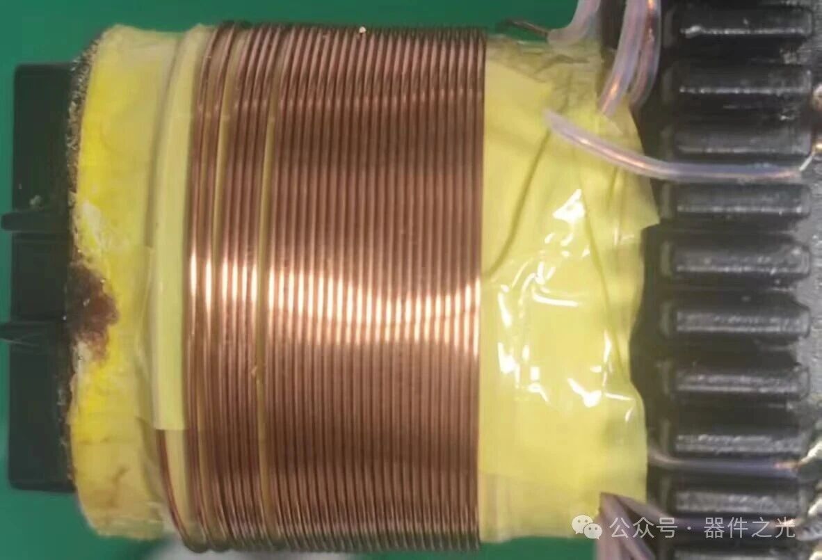
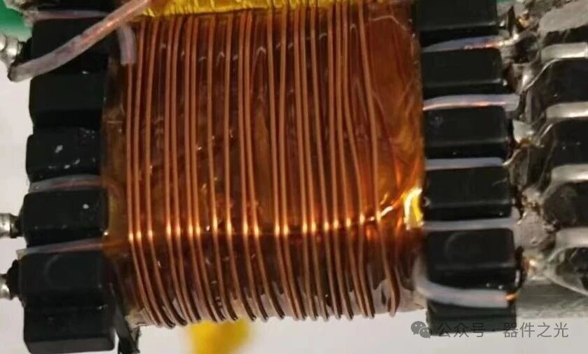
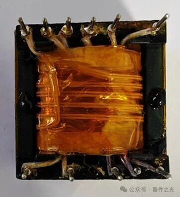
The distributed capacitance of transformer windings can be divided into four main parts:
(1) inter turn capacitance. A capacitor formed by the potential difference between adjacent turns. Although the capacitance value between single turns is small, repeated charging and discharging between turns may lead to insulation degradation and even breakdown and short circuit of enameled wire in high-voltage or high-power scenarios.
(2) Interlayer capacitance. The capacitance between different layers in the same winding. Interlayer capacitance is the main source of distributed capacitance, which forms an oscillation loop with leakage inductance at high frequencies, exacerbating electromagnetic interference problems and increasing voltage stress on the switching transistor.
3) Interwinding capacitance. The capacitance between primary and secondary, primary and VCC, and secondary and VCC windings. This capacitor provides a coupling path for common mode interference, which can cause noise from the primary side to be transmitted to the secondary side, affecting output stability.
(4) Stray capacitance. The capacitance of windings to magnetic cores, shielding layers, or casings is caused by factors such as circuit, structure, or layout. Although these capacitors are small, they may have an impact on high-frequency characteristics under specific layouts.
The distributed capacitance of transformer windings is often harmful, and its impact on circuits is as follows:
1. Electromagnetic compatibility issues. Distributed capacitance provides a coupling path between the primary and secondary windings, causing noise on the primary side to couple to the secondary side through capacitance, forming common mode interference and damaging the signal integrity of the circuit.
2. Decreased efficiency. Distributed capacitors in circuits can form capacitive currents, leading to an increase in reactive power of transformers and a decrease in overall efficiency. Secondly, the charging and discharging process of distributed capacitance increases additional losses, winding heating increases, and efficiency decreases.
3. Insulation damage. Distributed capacitance may cause local electric field concentration in high-voltage scenarios, leading to increased leakage current and even insulation material breakdown.
4. Decreased performance stability. Distributed capacitance and leakage inductance form a resonant circuit, causing voltage oscillation in the switching power supply, resulting in excessive voltage stress on the switching transistor and damage to the device.
In high-frequency applications, distributed capacitance can alter the equivalent circuit model of transformers, causing frequency response to deviate from the design value and affecting circuit stability. Distributed capacitance can also transmit switch noise to the output terminal through coupling, increasing power ripple and reducing output quality.
5. Design limitations and increased costs. To suppress the influence of distributed capacitance, it may be necessary to design additional RC buffer compensation circuits, which increases the complexity and cost of circuit design. In high-frequency scenarios, to reduce distributed capacitance, it may be necessary to use more expensive insulation materials and complex processes to design transformers, thereby increasing costs.
In high-frequency transformers, we can reduce the distributed capacitance of the transformer by increasing the distance between windings, increasing insulation thickness, using low dielectric constant insulation materials, improving winding methods, and increasing shielding layer design.
Post time: Nov-03-2025